Growth of III-V semiconductor nanowires (NWs) using the vapour-liquid-solid (VLS) method can result in crystal structures different from their bulk phase. In GaAs NWs, for example, stable zincblende (ZB) phase coexists with metastable wurtzite (WZ) structure. Controlling the crystal phase purity is critical for technological applications, because different crystal structures of the same chemical compound present different electronic, photonic or phononic properties, with discontinuities at their common interfaces. At the same time, controlled switching between the two phases enables synthesis of novel heterostructures with different electronic and optoelectronic properties in each phase. Remarkably, the valence and conduction bands of the two phases are misaligned, so that small sections of one phase within the other effectively confine charge carriers.
Using in situ TEM we image gallium arsenide (GaAs) and other III-V nanowires during growth as they switch between phases as a result of varying growth conditions. Combining these experimental results with theoretical investigation, we develop models to predict the phase change in III-V nanowires. We use this knowledge to engineer complex heterostructures composed by segments of different phases and for the fabrication of crystal-phase quantum dots having exceptional potential for application in photonics and quantum-computing.
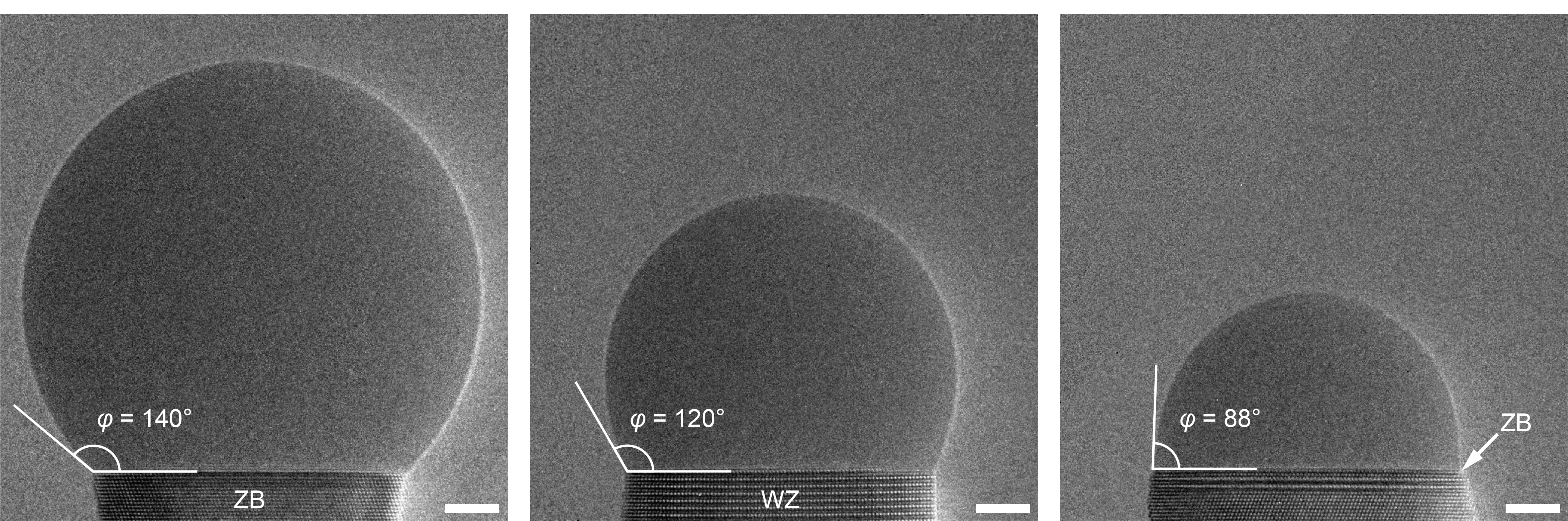
Figure 1. Growth mode and phase selection for a self-catalysed GaAs nanowire. The nanowire is growing at 420 °C under different fluxes of As and Ga. The As/Ga flux ratio was changed during growth to tune the volume of the catalyst droplet and consequently the contact angle (φ).
Left: ZB growing at large contact angle (φ > 125°). Center: WZ growing at intermediate contact angle (125° > φ > 100°). Right: ZB growing at small contact angle (φ < 100°). Scale bars are 5 nm. (Panciera et al. NanoLetters, 2020) Movie 1. Growth of ZB at large contact angles (φ > 125°). Growth of ZB NW section with an As flux of 0.06 nm/s and a Ga flux of 0.15 nm/s.
Each new ML grows quasi-instantaneously (in one frame) and its formation corresponds to the development of the edge truncation. The amount of truncation oscillates with the period of the monolayer (ML) growth, it decreases slowly but then jumps back to its maximum size with the next ML nucleation.
Note that the truncation appears simultaneously on both sides of the NW; asymmetric truncations are observed in the presence of stacking faults or near the transition from ZB to WZ. (Panciera et al. NanoLetters, 2020) Movie 2. Growth of WZ at intermediate contact angles (125° > φ > 100°). Growth of WZ NW section with an As flux of 0.08 nm/s and a Ga flux of 0.15 nm/s.
The edges of the wire are sharp (no truncation) and the step flows slowly across the planar top facet of the NW. (Unpublished) Movie 3. Growth of ZB at small contact angles (φ < 100°). Growth of ZB NW section with an As flux of 0.8 nm/s and Ga shutter closed.
Similarly to the WZ case (Movie2), the growth occurs by a slow step flow and the edge corner is sharp. (Panciera et al. NanoLetters, 2020)